LzEn
Junior Member

 Offline Offline
Posts: 78
Thank You
-Given: 48
-Receive: 86
Lazy Efficient
|
 |
« on: July 12, 2015, 03:54:00 15:54 » |
|
I have been testing this technique for a while now. At first I wast very skeptical about it but now that I have tested my boards for few months with this I think it is worth it to share with others. It is extremely easy to use with QFP, QFN, SOIC and TSSOP. The idea is to have a HASL board, align the component to the footprint, cover the pins with flux and heat everything up with the soldering iron. I know there are many concerns that not enough solder is there and the connection might not be good. But I did a lot of testing and so far so good. Sometimes I also put extra solder on the iron tip and go again just to be safe. I don't expect it to be used with boards that will be shipped to customers or anything. But for personal boards never had a problem. And here are some photos after the soldering is done. If anyone is interested here a quick video https://youtu.be/_vC16ZLQfHA. 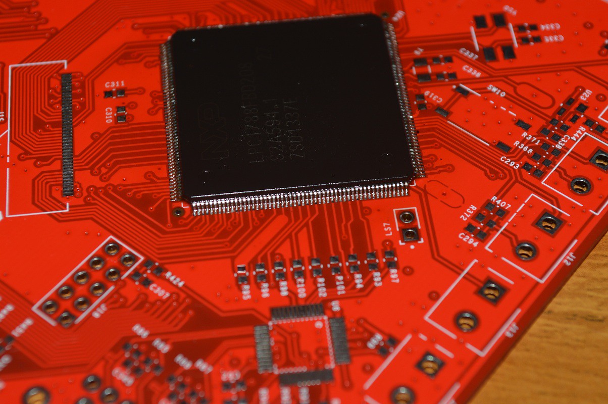 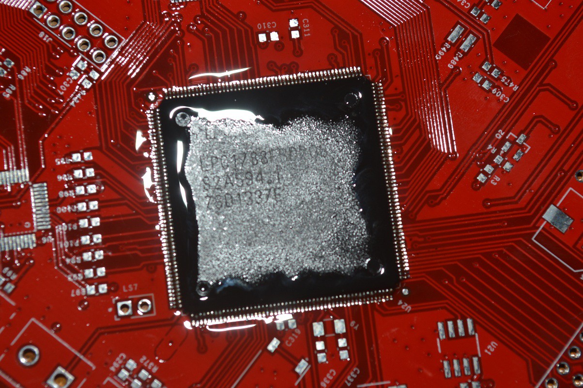  |
|
|
|
|
 Logged
|
~ Laziness Is The Mother Of Efficiency ~
|
|
|
CocaCola
Senior Member
Offline
Posts: 480
Thank You
-Given: 170
-Receive: 232
|
|
« Reply #1 on: July 12, 2015, 07:28:17 19:28 » |
|
I might use this to 'tack' the component (I know a lot of people that do this) but I would always properly solder afterwards... For me it's not worth dealing with the much higher potential for failure... That and all most of the boards I uses nowadays are gold not HASL...
|
|
|
|
|
Logged
|
|
|
|
crunx
Junior Member
Offline
Posts: 58
Thank You
-Given: 18
-Receive: 8
|
|
« Reply #2 on: July 12, 2015, 07:42:46 19:42 » |
|
The amount of tin in HASL s too low for a reliable connection to be formed. For hobby/prototype use I believe you can still get away with such substandard soldering fillet. Another matter is that use of gold (ENIG) finish gives better planarity than HASL, and for very small pitch parts that may also be an issue. And with gold you are lucky to get a good tack - all depending on amount of solder on the component's terminals. Here is a (relatively arbitrarily chosen) example how a solder joint should look like. You can't achieve this with HASL tin quantity only!  Of course, if you afterward hand-solder the pins adding some solder, it will be better. |
|
|
|
« Last Edit: July 13, 2015, 06:28:32 18:28 by crunx »
|
Logged
|
|
|
|
vern
V.I.P
Active Member
 Offline
Posts: 147
Thank You
-Given: 7
-Receive: 42
|
|
« Reply #3 on: July 12, 2015, 08:03:51 20:03 » |
|
It might work, but the pins need to have a very good coplanarity, because there is so little solder. If there is a gap of 1/10th of a millimeter the solder will not wet the pin and there will be no solder joint. You have to check very carefully (with a microscope) to see if everything is connected.
It is also very hard to solder BGA's that way, because the hight of the solder on each pad is different. As the BGA "swims" on on the pad with the most solder, other pads might not even touch the solder and are left unconnected.
With BGA's it is better to have a Gold plated board, because it is totally level. But here you can't solder any other components because the solder is missing.
But you can replace BGA's without adding extra solder paste, I have done that quite often.
|
|
|
|
|
Logged
|
|
|
|
CocaCola
Senior Member
Offline
Posts: 480
Thank You
-Given: 170
-Receive: 232
|
|
« Reply #4 on: July 12, 2015, 08:12:06 20:12 » |
|
One thing to note, very low cost laser Kapton (or even Mylar) screens can be had today so screening isn't nearly as costly as it used to be for the hobbyist... You can also find real metal generic multi-chip screens from Asia for dirt cheap, a nice addition to the tool box...
I have done multiple production runs of 500 units with nothing but a single Kapton screen and credit card, so I know they work well...
|
|
|
|
« Last Edit: July 13, 2015, 01:47:38 01:47 by CocaCola »
|
Logged
|
|
|
|
Checksum8
Active Member
Offline
Posts: 129
Thank You
-Given: 132
-Receive: 102
|
|
« Reply #5 on: July 12, 2015, 11:12:35 23:12 » |
|
You can also find real metal generic multi-chip screens from Asia for dirt cheap, a nice addition to the tool box...
CocaCola Do have any links or sources for these generic screens? I have not seen them for sale before. Thanks |
|
|
|
|
Logged
|
|
|
|
CocaCola
Senior Member
Offline
Posts: 480
Thank You
-Given: 170
-Receive: 232
|
|
« Reply #6 on: July 12, 2015, 11:49:04 23:49 » |
|
They can be found at most of the bigger Asian market websites like aliexpress under various names (lost in translation), for a few dollars delivered...
Try a Google search for 'cell phone soldering stencil' and start exploring the sites, many of the sellers that sell the phone stencils also offer up more generic stencils as well...
Most of them are obviously geared towards a particular device like a cell phone or game station and focus on BGA chips but even those come in use as component package layouts are generally universal... There are more generic ones out there as well for other chips... There are even kits to be found with 100s of individual component stencils...
Or you can do as I have and create your own generic stencils with the misc component packages you use a lot of the time, spaced out so they all have borders you can cut out , and have it produced...
|
|
|
|
« Last Edit: July 12, 2015, 11:51:40 23:51 by CocaCola »
|
Logged
|
|
|
|
LzEn
Junior Member
Offline
Posts: 78
Thank You
-Given: 48
-Receive: 86
Lazy Efficient
|
|
« Reply #7 on: July 13, 2015, 08:14:03 08:14 » |
|
I agree that this should probably be used for prototypes at home. Most of the times I tend to go ahead and add some solder to the joints after the parts is fixed in place.
My problem is that where I live there is mostly nothing available to buy (paste, stencil ...) and ordering from Aliexpress takes a longtime to arrive (+/- 45days) so I have to make something work with the tools I have thus this technique.
I don't think BGA is doable with the technique you need a re-flow oven to do that I guess and if you have that you better be doing it with stencil and paste.
|
|
|
|
|
Logged
|
~ Laziness Is The Mother Of Efficiency ~
|
|
|
CocaCola
Senior Member
Offline
Posts: 480
Thank You
-Given: 170
-Receive: 232
|
|
« Reply #8 on: July 13, 2015, 09:27:28 09:27 » |
|
I don't think BGA is doable with the technique you need a re-flow oven to do that I guess and if you have that you better be doing it with stencil and paste.
IMO as I said I don't believe it's realistically doable at all for any chip, a best you have a very poor solder joint that is bound to fail or cause other intermittent issues, especially as the device heats and cools... When I'm prototyping I don't any any intermittent issues or potential to fail joints, troubleshooting is hard enough without that concern... As I said many people use your trick to tack the chip in place for manual soldering, tack two opposite corners and then proceed to drag solder the other legs... This is exactly the way I was schooled to set and align chips when doing manual solder repairs and that was decades ago... |
|
|
|
|
Logged
|
|
|
|
LzEn
Junior Member
Offline
Posts: 78
Thank You
-Given: 48
-Receive: 86
Lazy Efficient
|
|
« Reply #9 on: July 13, 2015, 09:44:02 09:44 » |
|
When I'm prototyping I don't any any intermittent issues or potential to fail joints, troubleshooting is hard enough without that concern.. That is a very good point, you are right.. Even that I didn't face this problem with my testing but it is better to avoid this.. I will be using the flux as a first step as you mentioned and then go ahead and drag solder.. |
|
|
|
|
Logged
|
~ Laziness Is The Mother Of Efficiency ~
|
|
|
pickit2
Moderator
Hero Member
 Offline
Posts: 4684
Thank You
-Given: 859
-Receive: 4460
There is no evidence that I muted SoNsIvRi
|
|
« Reply #10 on: July 13, 2015, 11:31:58 11:31 » |
|
I like to use solder paste, an easy example you can adapt to suit your workbench shown here. https://www.youtube.com/watch?v=f_yFDpSTfao |
|
|
|
|
Logged
|
Note: I stoped Muteing bad members OK I now put thier account in sleep mode
|
|
|
LzEn
Junior Member
Offline
Posts: 78
Thank You
-Given: 48
-Receive: 86
Lazy Efficient
|
|
« Reply #11 on: July 13, 2015, 12:33:29 12:33 » |
|
Definitely a better connection at the joints.. I will give it a try on my next PCB.. |
|
|
|
|
Logged
|
~ Laziness Is The Mother Of Efficiency ~
|
|
|
mexpcb
Active Member
Offline
Posts: 124
Thank You
-Given: 35
-Receive: 211
|
|
« Reply #12 on: July 13, 2015, 11:09:59 23:09 » |
|
this is what i normally do...
i have solder all this types of packages (PLCC, QFN, QFP, SOT, TO, SO etc)..
1.- if you have a bare board (fresh new board), you have to place an small amount of solder using a lot of flux, then the pads will have an small amount of solder. Do this putting your board in an angle if possible.. if you are reworking, make sure there is no near components when you place it on an angle or find the one that will not interfere with the excess of solder, also just re touch the pads with flux and the hot tip
I normally use the spoon tips..
2.- after you have nice and clean solder in the pads, locate the component and just solder one of the pins on the corner, dont worry if it makes short with the closest ones, then go to the opposite corner and do the same..
At this stage make sure the pins on the corners are aligned..
3.- place your board on an angle and place enough flux on the pins. Start from top to bottom slicing the solder tip and the solder and slide it down slowly..
Make sure its hot enough..
4.- do the same on all the sides
. For soldering two sided pins its easier
Im success following this procedure even on QFNs
Regarding the video I dont see clearly the alignment, you can do that if you have four sides only using hot air or if you have good skills aligned that it may work, but for this particular package you have to align very well because when you move to the other sides the first one that gets soldered its already cold and soldered, then you cannot adjust it or move.. You can do it only if you apply hot by heating the entire surface and the component will align by itself
I hope it helps..
Regards
|
|
|
|
|
Logged
|
|
|
|
Elmer
Junior Member
Offline
Posts: 41
Thank You
-Given: 13
-Receive: 11
|
|
« Reply #13 on: July 14, 2015, 12:53:08 00:53 » |
|
Lots of nice tips here. I guess soldering is a bit like shaving, done in lots of different ways but rarely the topic of discussion... My $0.02:
When I'm lazy or have trouble going small enough (<=0.5mm pitch) I just go corners to hold in place, then solder the entire rows as a blob (lots of shorts) then i put an angled tip over wick to suck it up again. Works about 95%, you have to press each pin with a pointy tool to verify integrity, if pin moves resolder the single pin. Ofcourse I only do this on prototypes for test & demo, I don't do production soldering. The row blobs have high thermal conductivity iron->chip, so overheating the IC is a concern, I've tried it on those dense plastic type board-to-board connectors and alikes and they just melt so incredibly fast.
|
|
|
|
|
Logged
|
peace in the valley
|
|
|
LzEn
Junior Member
Offline
Posts: 78
Thank You
-Given: 48
-Receive: 86
Lazy Efficient
|
|
« Reply #14 on: July 14, 2015, 08:33:19 08:33 » |
|
this is what i normally do...
i have solder all this types of packages (PLCC, QFN, QFP, SOT, TO, SO etc)..
1.- if you have a bare board (fresh new board), you have to place an small amount of solder using a lot of flux, then the pads will have an small amount of solder. Do this putting your board in an angle if possible.. if you are reworking, make sure there is no near components when you place it on an angle or find the one that will not interfere with the excess of solder, also just re touch the pads with flux and the hot tip
I normally use the spoon tips..
2.- after you have nice and clean solder in the pads, locate the component and just solder one of the pins on the corner, dont worry if it makes short with the closest ones, then go to the opposite corner and do the same..
At this stage make sure the pins on the corners are aligned..
3.- place your board on an angle and place enough flux on the pins. Start from top to bottom slicing the solder tip and the solder and slide it down slowly..
Make sure its hot enough..
4.- do the same on all the sides
. For soldering two sided pins its easier
Im success following this procedure even on QFNs
Regarding the video I dont see clearly the alignment, you can do that if you have four sides only using hot air or if you have good skills aligned that it may work, but for this particular package you have to align very well because when you move to the other sides the first one that gets soldered its already cold and soldered, then you cannot adjust it or move.. You can do it only if you apply hot by heating the entire surface and the component will align by itself
I hope it helps..
Regards
What I understood is that you prepare the PCB and then you do drag soldering ? I didn't use any hot air in the video, I don't even have one.. The alignment is easy because I put a small drop of flux in the middle, this makes the whole chip a little stuck to the PCB. You can now easily align it with tweezers. Once you apply heat to the pins they tend to align themselves, never had alignment problems and I don't spend any time aligning. Just for reference : The chip in the video in case it is not clear from the photos is a 208 pins 0.5mm QFP LPC1788FBD208 Lots of nice tips here.
Couldn't agree more, a combination of all the above would make a great and easy soldering way |
|
|
|
|
Logged
|
~ Laziness Is The Mother Of Efficiency ~
|
|
|
Beltza
Junior Member
Offline
Posts: 82
Thank You
-Given: 228
-Receive: 42
|
|
« Reply #15 on: July 14, 2015, 09:13:03 09:13 » |
|
You can take a look at NASA soldering requirements. There you have a good reading time. |
|
|
|
|
Logged
|
|
|
|
|


