qwerty
Newbie

 Offline Offline
Posts: 14
Thank You
-Given: 59
-Receive: 1
|
 |
« on: July 24, 2007, 01:56:19 13:56 » |
|
|
|
|
|
|
 Logged
|
|
|
|
hate
Hero Member
Offline
Posts: 551
Thank You
-Given: 156
-Receive: 355
|
|
« Reply #1 on: July 24, 2007, 05:43:49 17:43 » |
|
Try connecting Vee to GND!
Regards...
|
|
|
|
|
Logged
|
Regards...
|
|
|
jeanninemtv
Senior Member
Offline
Posts: 311
Thank You
-Given: 57
-Receive: 25
|
|
« Reply #2 on: July 25, 2007, 04:15:11 04:15 » |
|
attach voltages to the opamps... your power rails are not in the sheet.....
please never forget to put it,,,,
put power pin with +12V and -12V .. then check if your opamps have model . or lisa file...
and then press run....
you will have good simulation, i hope-..
|
|
|
|
|
Logged
|
|
|
|
qwerty
Newbie
Offline
Posts: 14
Thank You
-Given: 59
-Receive: 1
|
|
« Reply #3 on: July 25, 2007, 07:22:52 07:22 » |
|
thanks for the reply.  how to attach the voltages to the opamps? the device for U2 in the library doesn't show any pin to attach. is this correct to put in the schematics for voltage supply? 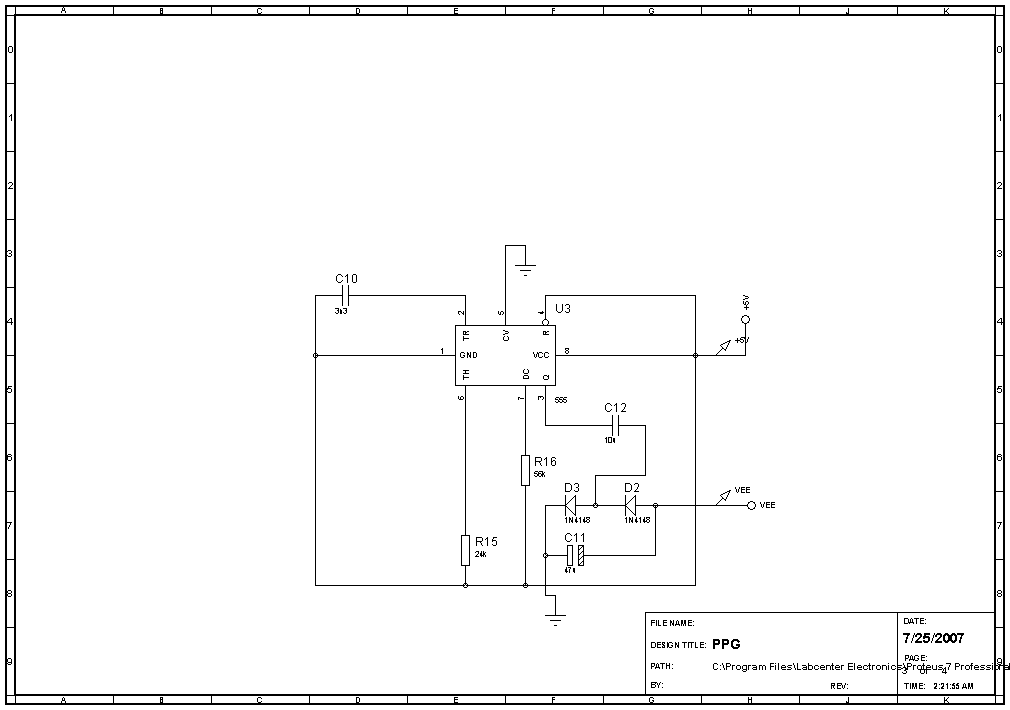 when i stimulate it shows this problem 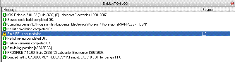 and for the Erc check ELECTRICAL RULES CHECK REPORT ============================= Design: PPG Doc. no.: <NONE> Revision: <NONE> Author: <NONE> Created: 07/21/07 Modified: 07/25/07 #I:Compiling design 'C:\Program Files\Labcenter Electronics\Proteus 7 Professional\SAMPLES\project.DSN'. %C=0002,00000003 WARNING: U2,Y0 (I/O) connected toU1:C,OP (Output) WARNING: U2,X0 (I/O) connected toU1:D,OP (Output) WARNING: U1:D,OP (Output) connected toU2,X1 (I/O) WARNING: GND,<TERM> (Power Rail) connected toU2,Z0 (I/O) WARNING: VSS,<TERM> (Power Terminal) connected toU2,Z0 (I/O) WARNING: U2,VSS (Power Pin) connected toU2,Z0 (I/O) WARNING: U1:D,V- (Power Pin) connected toU2,Z0 (I/O) WARNING: U1:C,V- (Power Pin) connected toU2,Z0 (I/O) WARNING: U2,Z0 (I/O) connected toU1:B,V- (Power Pin) WARNING: U2,Z0 (I/O) connected toU1:A,V- (Power Pin) Netlist generated OK. ERC errors found. |
|
|
|
« Last Edit: July 25, 2007, 07:24:45 07:24 by qwerty »
|
Logged
|
|
|
|
hate
Hero Member
Offline
Posts: 551
Thank You
-Given: 156
-Receive: 355
|
|
« Reply #4 on: July 25, 2007, 08:52:09 08:52 » |
|
Create a 'Power Terminal', type in 'VEE' and tie it to GND so the 'VEE' pin of IC 'U2' should be connected to GND now! Alternatively you can change the connection of the power pins of an IC from properties menu, double click on the device to enter properties dialog and you'll see the 'hidden pins' button. Use it to tie the hidden pins to wherever you want!
Regards...
|
|
|
|
|
Logged
|
Regards...
|
|
|
qwerty
Newbie
Offline
Posts: 14
Thank You
-Given: 59
-Receive: 1
|
|
« Reply #5 on: July 25, 2007, 10:55:15 10:55 » |
|
thank you so much for replying. thanks. i tried making a power rail VEE to connect to GND like this 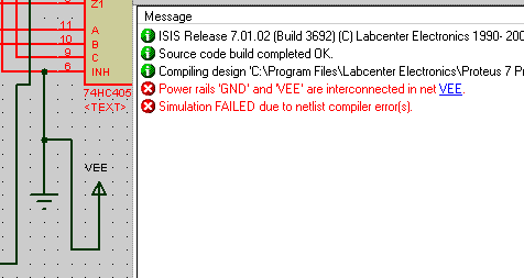 it shows that error when stimulate. and i tried changing the hidden pins like this, am i correct ? 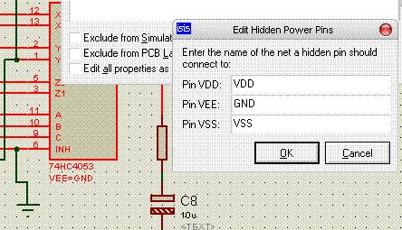 but when stimulate it still shows the same error, T_T.. anyone have tried drawing this schematics? thanks again. |
|
|
|
« Last Edit: July 25, 2007, 10:56:57 10:56 by qwerty »
|
Logged
|
|
|
|
hate
Hero Member
Offline
Posts: 551
Thank You
-Given: 156
-Receive: 355
|
|
« Reply #6 on: July 25, 2007, 11:33:36 11:33 » |
|
I analyzed your schematic carefully and I see that VEE shouldn't be tied to GND because there should be a negative voltage on that pin. So the default configuration is ok, don't tie it to GND, in the 'Configure Power Rails' menu under 'Design' menu it is connected to '-5v', check this first! The 'Pin 'VEE' is not modelled.' is not an error it's a warning so it simulates the schematic but with wrong behavior as I guess from your post. Please be sure about that! If it doesn't even simulate then there is another main problem to be solved.
Regards...
|
|
|
|
|
Logged
|
Regards...
|
|
|
qwerty
Newbie
Offline
Posts: 14
Thank You
-Given: 59
-Receive: 1
|
|
« Reply #7 on: July 25, 2007, 12:20:13 12:20 » |
|
using the default configuration , in the configure power rails menu , the VEE shows that it is connected to -5v. the circuit can be stimulate , only it shows that the pin VEE is not modelled only. and ERC error like this..
ELECTRICAL RULES CHECK REPORT
=============================
Design: PPG
Doc. no.: <NONE>
Revision: <NONE>
Author: <NONE>
Created: 07/21/07
Modified: 07/25/07
#I:Compiling design 'C:\Program Files\Labcenter Electronics\Proteus 7 Professional\SAMPLES\ppg.DSN'.
%C=0002,00000003
WARNING: U2,Y0 (I/O) connected toU1:C,OP (Output)
WARNING: U2,X0 (I/O) connected toU1:D,OP (Output)
WARNING: U1:D,OP (Output) connected toU2,X1 (I/O)
WARNING: GND,<TERM> (Power Rail) connected toU2,Z0 (I/O)
WARNING: VSS,<TERM> (Power Terminal) connected toU2,Z0 (I/O)
WARNING: U2,VSS (Power Pin) connected toU2,Z0 (I/O)
WARNING: U1:D,V- (Power Pin) connected toU2,Z0 (I/O)
WARNING: U1:C,V- (Power Pin) connected toU2,Z0 (I/O)
WARNING: U2,Z0 (I/O) connected toU1:B,V- (Power Pin)
WARNING: U2,Z0 (I/O) connected toU1:A,V- (Power Pin)
Netlist generated OK.
ERC errors found.
how to correct this error? is it my connection is wrong?
thanks for helping.
best regards,
|
|
|
|
|
Logged
|
|
|
|
hate
Hero Member
Offline
Posts: 551
Thank You
-Given: 156
-Receive: 355
|
|
« Reply #8 on: July 25, 2007, 05:53:57 17:53 » |
|
Sorry but I can't see the error, all of them are warnings! If you can post the '.dsn' file I can try to simulate also but not much I can do with this data.
Regards...
|
|
|
|
|
Logged
|
Regards...
|
|
|
qwerty
Newbie
Offline
Posts: 14
Thank You
-Given: 59
-Receive: 1
|
|
« Reply #9 on: July 26, 2007, 12:55:10 00:55 » |
|
|
|
|
|
« Last Edit: July 26, 2007, 01:12:31 01:12 by qwerty »
|
Logged
|
|
|
|
hate
Hero Member
Offline
Posts: 551
Thank You
-Given: 156
-Receive: 355
|
|
« Reply #10 on: July 26, 2007, 09:24:15 09:24 » |
|
In the 3rd sheet, the one with 555(U3) both 'GND' and '+5V' are tied together! This needs to be corrected first, and what does this 555 needed for, to create a -V supply or something else please explain?
Regards...
|
|
|
|
|
Logged
|
Regards...
|
|
|
qwerty
Newbie
Offline
Posts: 14
Thank You
-Given: 59
-Receive: 1
|
|
« Reply #11 on: July 26, 2007, 10:26:23 10:26 » |
|
ah , sorry2.. that 3rd circuit was just for testing , cause i thought VEE should have -5v, so i tried making that circuit. i think that circuit could be ignored 1st. sorry again.
the problem is at the 1st and 2nd sheet only. i forgot to delete the 3rd one.
thanks.
|
|
|
|
|
Logged
|
|
|
|
hate
Hero Member
Offline
Posts: 551
Thank You
-Given: 156
-Receive: 355
|
|
« Reply #12 on: July 26, 2007, 12:07:45 12:07 » |
|
Ok I'll try it without the 3rd sheet again, but I still can't find any lethal error with simulating still searching!
Regards...
|
|
|
|
|
Logged
|
Regards...
|
|
|
qwerty
Newbie
Offline
Posts: 14
Thank You
-Given: 59
-Receive: 1
|
|
« Reply #13 on: July 26, 2007, 01:27:09 13:27 » |
|
hurmm , maybe the ERC error , is just a warning only ? does'nt affect the circuit function?
|
|
|
|
|
Logged
|
|
|
|
hate
Hero Member
Offline
Posts: 551
Thank You
-Given: 156
-Receive: 355
|
|
« Reply #14 on: July 26, 2007, 06:23:10 18:23 » |
|
No errors again! What should be there at the input of the transistor Q5 at 1st sheet?
Regards...
|
|
|
|
|
Logged
|
Regards...
|
|
|
qwerty
Newbie
Offline
Posts: 14
Thank You
-Given: 59
-Receive: 1
|
|
« Reply #15 on: July 26, 2007, 09:16:50 21:16 » |
|
it suppose to have a HLC1395-001 here's the datasheet. http://www.farnell.com/datasheets/25067.pdf The HLC1395 is a miniature infrared sensor designed to sense reflective objects at short distances. but i can't find a suitable model for it. so i just draw it according to the schematics. thanks |
|
|
|
|
Logged
|
|
|
|
hate
Hero Member
Offline
Posts: 551
Thank You
-Given: 156
-Receive: 355
|
|
« Reply #16 on: July 27, 2007, 01:14:57 01:14 » |
|
Ok but you have to use something to simulate there otherwise don't expect any simulation results, try to inject a signal generator there and see what happens.
Regards...
|
|
|
|
|
Logged
|
Regards...
|
|
|
|
|
hate
Hero Member
Offline
Posts: 551
Thank You
-Given: 156
-Receive: 355
|
|
« Reply #18 on: July 27, 2007, 03:23:12 15:23 » |
|
You don't have to apply exactly the same signal there, just apply something similar and don't go on adding more parts without getting acceptable results from what you have!
Regards...
|
|
|
|
|
Logged
|
Regards...
|
|
|
|


