Sonsivri
 
*
Welcome, Guest. Please login or register.
Did you miss your activation email?
April 20, 2024, 11:52:13 11:52


Login with username, password and session length


Pages: [1]
Print
Author Topic: "Dual-purpose" pins on Cyclone II FPGA and Quartus II behavior question  (Read 4137 times)
0 Members and 1 Guest are viewing this topic.
Just4Fun
Newbie
*
Offline Offline

Posts: 21

Thank You
-Given: 6
-Receive: 20


« on: January 19, 2019, 12:07:09 12:07 »

Hi,
I've designed an "homemade" FPGA dev board (EP2C5T144C8N based) and I'm currently making the first tests.
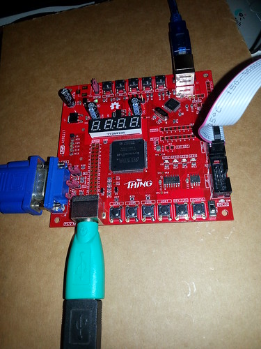
I've used one of the "dual-purpose" FPGA pins to drive a LED too (see LED4 on the attachment jpg). The FPGA pin is ASDO.
The board uses an EPCS4 as eeprom in AS mode.


In the Cyclone datasheet (ehm... they call it "handbook"...) they says that the "dual-purpose" pins can be used as normal I/O after configuration if JTAG is used (not if AS is used).
More, there is a bug in Quartus II v13sp1 (the last one version that supports Cyclone II) on the "dual-purpose" pins and you have to chose "Passive Serial" mode when compiling to avoid an error (when using JTAG to transfer the bitstream to the FPGA the AS or PS mode selection is irrelevant...).

I'm able to compile and transfer the bitstream successfully (and without any error in the compile phase) to the FPGA using JTAG, but the Led on the ASDO pin doesn't turn on.
More, in the Quartus II fitter output the ASDO line seems correctly set as an user I/O output pin...
I'm sure that the Led works because in the AS mode, when the FPGA loads the bitstream from the EPCS4 eeprom, that Led is active showing the load phase.

Anyone has experimented anything about this (I haven't found any indication on the Altera/Intel forum or docs about this, and I know that is very "specific", but I'm curious...)?


BTW: In the second attachment there is the part of the Cylone II Hanbook (https://www.intel.com/content/dam/www/programmable/us/en/pdfs/literature/hb/cyc2/cyc2_cii5v1.pdf Table 13–11) that says that it is possible...


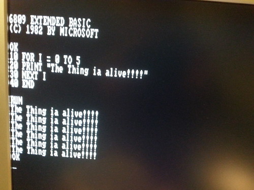
BTW2: Of course I'll publish here all the details when fully tested... Up to now it seems to work.. here "running" a SOC with a 6809 CPU, Basic ROM, some RAM , VDU and PS/2 Kb. controller (sorry for the typo...):


« Last Edit: January 19, 2019, 12:59:54 12:59 by Just4Fun » Logged
h0nk
Senior Member
****
Offline Offline

Posts: 256

Thank You
-Given: 208
-Receive: 230


« Reply #1 on: January 19, 2019, 08:02:47 20:02 »


Hello Just4Fun,

You can configure the behaviour of "Dual-Purpose Pins" with the "Device and Pin Options" of  Your project.
ASDO is configured together with nCSO "As input tri-stated" or as "Use as regular I/O".

For a general purpose board i would not mess with this signals. ASDO is connected to ASDI of the
configflash and NCSO to nCS.
If someone wish to store more information beyond the configuration bitstream (e.g. NIOS2 Flash)
the configflash would not readable.


Best Regards
Logged
Just4Fun
Newbie
*
Offline Offline

Posts: 21

Thank You
-Given: 6
-Receive: 20


« Reply #2 on: January 20, 2019, 11:38:29 11:38 »

Hi h0nk,

You can configure the behaviour of "Dual-Purpose Pins" with the "Device and Pin Options"...

it's exactly what I've done...

For a general purpose board i would not mess with this signals. ASDO is connected to ASDI of the
configflash and NCSO to nCS...

Yes.. I completely agree with you.. ASDO and nCSO are very "sensible" control signals...
However because I placed a led on the ASDO line to show the activity on the EPCS4 eeprom (and it works fine) I only wanted to test what the datasheet says... and yes... I'm too much curious...   Smiley

After all I can live happy with this... probably it is a Quartus II v13sp1 problem... so the only way should be give a look at low level in the bitstream... but this is an other story...
Logged
h0nk
Senior Member
****
Offline Offline

Posts: 256

Thank You
-Given: 208
-Receive: 230


« Reply #3 on: January 20, 2019, 04:01:04 16:01 »

Hello Just4Fun,

i made some Test with various QuartusII Versions:

With Quartus 9.1 there is no choice: "Use as regular I/O"
Only "As input tri-stated".

With Quartus 11.1 SP2 i could: "Use as regular I/O",
but only together with "Passive Serial" as Configuration Device.
With "Active Serial":
Error (176310): Can't place multiple pins assigned to pin location Pin_1 (IOC_X0_Y13_N0)

With my board i am unable to start the FPGA without the configflash.
So ASDO is already configured in some way before JTAG comes in.

If you want to test: Remove the connection from ASDO of the configflash
to your circuit and generate a bitstream for a "Passive Serial" Configdevice
and write this via JTAG to Your FPGA.

Its only a test to proof that ASDO is a "normal" IO-Pin after rhis.
But JTAG is not the normal way to configure the FPGA.
With a EPC4 this would be "Active Serial".


Best Regards
Logged
Just4Fun
Newbie
*
Offline Offline

Posts: 21

Thank You
-Given: 6
-Receive: 20


« Reply #4 on: January 21, 2019, 12:55:45 12:55 »

Hi h0nk,

With Quartus 11.1 SP2 i could: "Use as regular I/O",
but only together with "Passive Serial" as Configuration Device.
With "Active Serial":
Error (176310): Can't place multiple pins assigned to pin location Pin_1 (IOC_X0_Y13_N0)

This is the same result I get with Quartus II v13sp1.
Altera/Intel (or now Intel only...) says that it is a Quartus II bug and to set Passive Mode as you and me did for a successful compilation (see this Intel note:
https://www.intel.com/content/www/us/en/programmable/support/support-resources/knowledge-base/solutions/rd06252012_419.html)

If you want to test: Remove the connection from ASDO of the configflash
to your circuit and generate a bitstream for a "Passive Serial" Configdevice
and write this via JTAG to Your FPGA.

This is a good idea...  Smiley Next board I assemble I'll leave the EPS4 unpopulated so I can do this test.
I'll post here any further result.

But JTAG is not the normal way to configure the FPGA.
With a EPC4 this would be "Active Serial".

Yes, but I can test a bitstrem with JTAG without write it into the configflash, and than write it into the configflash with the JTAG mode and connector using the SFL IP core as well explained here: https://www.youtube.com/watch?v=dPSFCGNQOCU
I've tested this way and it worked (I mean the configflash write, not the use of ASDO as IO pin...)!
Of course after the write operation you must load the bitstream asserting the nCONFIG signal, and it will be loaded in AS mode.

Best regards.
J4F
« Last Edit: January 21, 2019, 01:41:45 13:41 by Just4Fun » Logged
Just4Fun
Newbie
*
Offline Offline

Posts: 21

Thank You
-Given: 6
-Receive: 20


« Reply #5 on: February 19, 2019, 08:29:37 08:29 »

Just to complete the info, as suggested by h0nk, I've made a new test on a new board without the EPCS4 eeprom soldered.

But the behavior was the same... at compile time all seems ok, but anyway the ASDO pin didn't work as an IO pin ... (using JTAG to program the configuration).

So or there is a "bug" in Quartus II (v13sp1), or when MEMSEL0/1 are set in the AS/JTAG mode (both LOW. See the attachment in my first post) the ASDO pin can't be used as IO in any case (and the datasheet is not clear about this...).
« Last Edit: February 19, 2019, 08:43:14 08:43 by Just4Fun » Logged
Pages: [1]
Print
Jump to:  


DISCLAIMER
WE DONT HOST ANY ILLEGAL FILES ON THE SERVER
USE CONTACT US TO REPORT ILLEGAL FILES
ADMINISTRATORS CANNOT BE HELD RESPONSIBLE FOR USERS POSTS AND LINKS

... Copyright © 2003-2999 Sonsivri.to ...
Powered by SMF 1.1.18 | SMF © 2006-2009, Simple Machines LLC | HarzeM Dilber MC