mr_byte31
Hero Member

 Offline Offline
Posts: 594
Thank You
-Given: 68
-Receive: 144
|
 |
« on: March 06, 2024, 10:18:58 10:18 » |
|
Hi Folks, I need some support for this circuit: The first stage has 20x gain and second stage has 21x gain. The overall gain is 20x21 = 400 aprox. 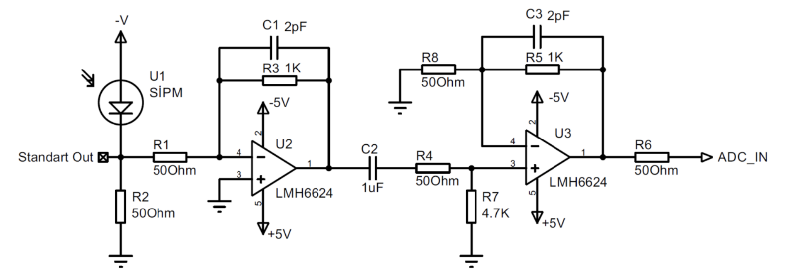 I tried to implement it on NI MultiSim (simulation file is attached): I substituted the photodiode with pulsed current source (100ns pulse width, 1 microampere) 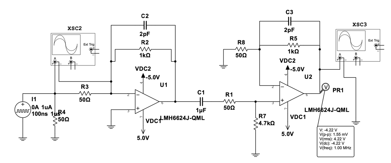 I tried to increase the gain of the amplifier so I increased the feedback resistance of the both stages to be (10K). I noticed that the output of the last stage become lower !!! is there any explanation for that ? |
|
|
|
« Last Edit: March 06, 2024, 10:30:16 10:30 by mr_byte31 »
|
 Logged
|
Do not trifle with the Moderators , as you are small, and crunchy, and taste good with ketchup.
|
|
|
Sideshow Bob
Cracking Team
Hero Member
Offline
Posts: 985
Thank You
-Given: 230
-Receive: 961
|
|
« Reply #1 on: March 06, 2024, 10:45:35 10:45 » |
|
  Have you run any frequency analysis Also you may find this link interesting https://www.ti.com/lit/sboa293
|
|
|
|
|
Logged
|
I have come here to chew bubblegum and kick ass... and I'm all out of bubblegum
|
|
|
mr_byte31
Hero Member
Offline
Posts: 594
Thank You
-Given: 68
-Receive: 144
|
|
« Reply #2 on: March 06, 2024, 10:52:28 10:52 » |
|
I made AC analysis, the circuit show flat magnitude till 800MHz
whats the point ?
|
|
|
|
|
Logged
|
Do not trifle with the Moderators , as you are small, and crunchy, and taste good with ketchup.
|
|
|
dennis78
Active Member
Offline
Posts: 121
Thank You
-Given: 268
-Receive: 153
|
|
« Reply #3 on: March 06, 2024, 01:27:30 13:27 » |
|
First: AC analysis is not relevant for transient results because: 1. different models used for same part (transient vs ac models) 2. as is relevant for specific dc conditions - small signal analysis (small relative to dc bias). 3.... Second (it is only about sim, not relevant for real circuit): I try your circuit and see when you increase gain it produce big offset error so your amplifier go to saturation -> signal became limited -> it is reason for lower results. First modify your circuit to decrease dc offset. In real case this will not work as on sim, you need frequency compensation network for higher(and stable) gains and in it case you will possible get limited results because of many other reasons. Sorry for my bad English  |
|
|
|
« Last Edit: March 06, 2024, 02:18:15 14:18 by dennis78 »
|
Logged
|
|
|
|
PM3295
Senior Member
 Online Online
Posts: 279
Thank You
-Given: 340
-Receive: 132
|
|
« Reply #4 on: March 06, 2024, 07:32:22 19:32 » |
|
As mentioned, the DC offset of the last stage will be a problem. With your rise/fall-time settings of 1 ns, the 2 pF stray capacitance will also be problematic with the higher gain feedback values.
|
|
|
|
|
Logged
|
|
|
|
PM3295
Senior Member
Online
Posts: 279
Thank You
-Given: 340
-Receive: 132
|
|
« Reply #5 on: March 07, 2024, 01:32:51 01:32 » |
|
You can achieve good results if you add a current feedback amplifier in the feedback loop of each amplification stage. Then you can also split the resistors into multiple sections to reduce the stray capacitance associated with each part. Since you are dealing with very fast amplifiers, layout will be critical for performance and stability. The modified circuit shown, produce a 1 Vpp out for your stated input. The DC offset is corrected with adjusting R18.
I have included the project files in Proteus and Multisim formats for those who want to play with it.
Note: Signal on chan A in Proteus appears to show zero because the pulse amplitude is only 25 uVpp.
|
|
|
|
« Last Edit: March 07, 2024, 01:49:30 01:49 by PM3295 »
|
Logged
|
|
|
|
PM3295
Senior Member
Online
Posts: 279
Thank You
-Given: 340
-Receive: 132
|
|
« Reply #6 on: March 07, 2024, 03:34:35 03:34 » |
|
The graph simulation results in Proteus show Vin and Vout more clearly.
|
|
|
|
|
Logged
|
|
|
|
mr_byte31
Hero Member
Offline
Posts: 594
Thank You
-Given: 68
-Receive: 144
|
|
« Reply #7 on: March 07, 2024, 01:47:20 13:47 » |
|
The DC offset was the source of all my problems. Many thanks for the hint. I tried to add a capacitor (C4) at the negative terminal of the second stage. I ran the simulation and it went fine !! I was thinking that C4 will block any DC voltage to be amplified. what's your opinion ? 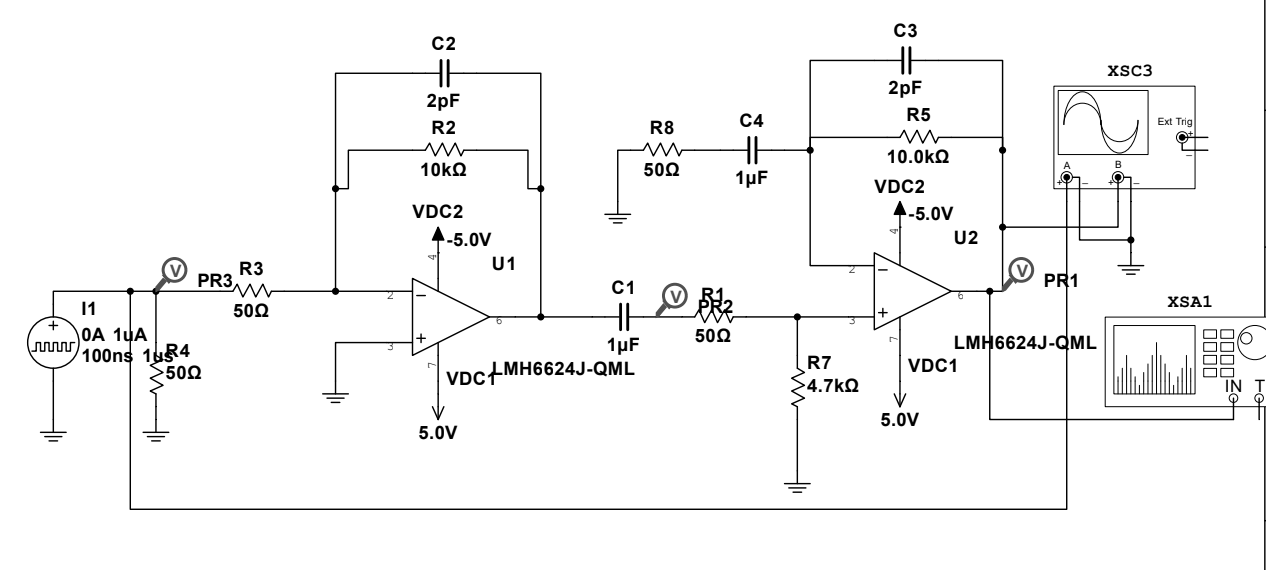 |
|
|
|
|
Logged
|
Do not trifle with the Moderators , as you are small, and crunchy, and taste good with ketchup.
|
|
|
PM3295
Senior Member
Online
Posts: 279
Thank You
-Given: 340
-Receive: 132
|
|
« Reply #8 on: March 07, 2024, 03:03:42 15:03 » |
|
Inserting the capacitor may work for the DC offset, but the type and quality of the capacitor may be an issue for precise amplification. If you look at the comparison between your latest circuit and my modified circuit, you see the obvious problems. The AC gain is affected by the capacitor, and the problem with parasitic/stray capacitance causes pulse shapes that are far from the original.
I find it useful to have some form of adjustable DC shift control of the output signal.
|
|
|
|
|
Logged
|
|
|
|
mr_byte31
Hero Member
Offline
Posts: 594
Thank You
-Given: 68
-Receive: 144
|
|
« Reply #9 on: March 14, 2024, 04:39:08 16:39 » |
|
@PM3295, your circuit is much better than mine ! I didn't study this kind of topology in university so I was surprised that you put a feedback from second OPAMP to first one. do you have any material that I can study more to understand your circuit ? one more question : is there any IC that can do this all this amplifications and automatic gain control for me ? I found MC1350P but it is IF amplifier. |
|
|
|
|
Logged
|
Do not trifle with the Moderators , as you are small, and crunchy, and taste good with ketchup.
|
|
|
PM3295
Senior Member
Online
Posts: 279
Thank You
-Given: 340
-Receive: 132
|
|
« Reply #10 on: March 14, 2024, 07:03:12 19:03 » |
|
I didn't study this kind of topology in university so I was surprised that you put a feedback from second OPAMP to first one.
do you have any material that I can study more to understand your circuit ?
I don't have any reading material on this, but this technique is often used in designing amplifiers for mass-spectrometry, where you deal with very high gains, which reduces the amplifier bandwidth. The CFA helps to improve the final slewrate of the amplifier stage. The slewrate of the CFA should be at least ten times that of the VFA. If you search papers on pulse amplifiers for mass-spectrometry, you may find something. |
|
|
|
|
Logged
|
|
|
|
|


