promach
Junior Member

 Offline Offline
Posts: 44
Thank You
-Given: 14
-Receive: 0
|
 |
« on: February 22, 2016, 03:05:29 15:05 » |
|
Hi all,
I have a personal target as well as school project work to develop an op-amp based on performance specifications with LTspice simulation.
Please do not regard this as totally asking for solution (this is purely for learning purpose and finish electronic project work within timeline).
I am open to new design which I have not learnt before. I have only dealt with 741-opamp internal circuitry for a month.
Performance specifications are like the following:
a) Power dissipation <3mW
b) DC small signal gain >80dB
c) Unity gain bandwidth >50MHz
d) Settling time <25ns to 0.1% for both rise and fall
e) Input common mode range +1.5 +- 0.5V
f) Output swing >1.6V
g) Phase margin >60 deg with 5pF load
h) Power Supply Rejection Ratio (PSRR) >80dB at DC
i) Common Mode rejection at DC (CMRR) >80dB at +1.5V common mode
All MOS devices are qualified to 3V
Setting time is measured with a step input of 0.5V (1.25V to 1.75V) when configured as a unity gain voltage follower and a load capacitance of 500fF
How should start about ?
I am learning about two-stage opamp but I am not sure how to relate to the performance spec.
|
|
|
|
|
 Logged
|
|
|
|
optikon
Cracking Team
Hero Member
Offline
Posts: 848
Thank You
-Given: 1092
-Receive: 2000
|
|
« Reply #1 on: February 22, 2016, 11:06:52 23:06 » |
|
One approach is to put together a typical design so you have something to work from and then check each of your parameter. As you find they do or do not meet what you need, you can make adjustments accordingly. Only with vast experience will you have a a good knowledge of which architecture choices will be best for the design.
Start with what you know about the 741 design converted to MOS technology and see how it performs.
Also check that you know the proper definition of each parameter you are asked to meet.
|
|
|
|
« Last Edit: February 22, 2016, 11:13:02 23:13 by optikon »
|
Logged
|
I can explain this to you. I can't comprehend it for you.
|
|
|
Vineyards
Active Member
Offline
Posts: 168
Thank You
-Given: 62
-Receive: 37
|
|
« Reply #2 on: February 23, 2016, 02:46:28 14:46 » |
|
You need a newer opamp that can operate at plus/minus 3.3V-5V range preferably a rail-to-rail one.
Because 741 doesn't have enough unity gain bandwith (1MHz) and other commonly available chips usually offer a few times as much bandwith as it does. (e.g. TL081 s.t. like 4MHz). Ca3140 could satisfy this parameter but it is a very old chip. PSSR and CMMR should not be a problem. Even many of the simplest opamps can go beyond the required value.
|
|
|
|
|
Logged
|
|
|
|
Parmin
Hero Member
Offline
Posts: 582
Thank You
-Given: 494
-Receive: 133
Very Wise (and grouchy) Old Man
|
|
« Reply #3 on: February 23, 2016, 09:13:35 21:13 » |
|
I would probably go to DIGIKEY or Mouser website and plunk in the parameters on the search link
|
|
|
|
|
Logged
|
If I have said something that offends you, please let me know, so I can say it again later.
|
|
|
optikon
Cracking Team
Hero Member
Offline
Posts: 848
Thank You
-Given: 1092
-Receive: 2000
|
|
« Reply #4 on: February 23, 2016, 10:05:59 22:05 » |
|
It sounds to me like the OP is asking about designing an opamp (from transistors!)... not designing with an opamp...
If designing opamp from scratch the standard reference design is a 741 which is good for beginners..
if you are designing circuits WITH opamps, the 741 is terrible choice.
|
|
|
|
|
Logged
|
I can explain this to you. I can't comprehend it for you.
|
|
|
PICker
Active Member
Offline
Posts: 162
Thank You
-Given: 207
-Receive: 109
|
|
« Reply #5 on: February 24, 2016, 02:25:29 02:25 » |
|
I agree with optikon and I think promach is looking for an opamp design guide ("designing an opamp"). While it is relatively easy to find material about designing with opamps, it is no so easy to find how design opamps. Try this link to some basic youtube videos about opamps design with Cadence: https://www.youtube.com/watch?v=Qbx0YI6UjoE&list=PLK2eyR1C9gjrMCVXRvKhY7CjNZYGCgMnY |
|
|
|
|
Logged
|
|
|
|
TucoRamirez
Senior Member
Offline
Posts: 307
Thank You
-Given: 257
-Receive: 115
Tuco ... dead or Alive
|
|
« Reply #6 on: February 24, 2016, 07:24:33 07:24 » |
|
On wich design kit are you working? 350nm? 130nm? it will help you a lot to know that for transistor sizing
|
|
|
|
|
Logged
|
Whoever double crosses me and leaves me alive... he understands nothing about Tuco.
|
|
|
promach
Junior Member
Offline
Posts: 44
Thank You
-Given: 14
-Receive: 0
|
|
« Reply #7 on: February 24, 2016, 03:30:34 15:30 » |
|
it is 0.18µm CMOS process. Besides, I can only use ONE ideal current source. The extra requirement (generate all voltage and current biases without using ideal current source) would be impossible for me.
|
|
|
|
|
Logged
|
|
|
|
TucoRamirez
Senior Member
Offline
Posts: 307
Thank You
-Given: 257
-Receive: 115
Tuco ... dead or Alive
|
|
« Reply #8 on: February 24, 2016, 09:32:11 21:32 » |
|
do you have some base parameters of your process to do your sizing calculations (kn, kp, gm/Id courbes etc)?
|
|
|
|
|
Logged
|
Whoever double crosses me and leaves me alive... he understands nothing about Tuco.
|
|
|
promach
Junior Member
Offline
Posts: 44
Thank You
-Given: 14
-Receive: 0
|
|
« Reply #9 on: February 25, 2016, 12:32:40 00:32 » |
|
I am already given a library(.lib) with pmos and nmos symbols (.asy). Are these what you mean ? Besides, what it means by "DC small signal gain" ? From http://microchip.wikidot.com/asp0107:output-voltage-swing, Output Voltage Swing defines how close the op-amp output can be driven to rail to rail. So, what does it mean by the output swing of > 1.6V ? |
|
|
|
« Last Edit: February 25, 2016, 01:44:23 01:44 by promach »
|
Logged
|
|
|
|
crunx
Junior Member
Offline
Posts: 58
Thank You
-Given: 18
-Receive: 8
|
|
« Reply #10 on: February 25, 2016, 05:30:27 05:30 » |
|
If you plan to design n opamp from scratch - using transistors on an IC, the project is something else... and I have no experience in design of analog silicon chips. However, if you would like to try to build an amplifier using existing opamp ICs, I have some experience. I assume the latter below.
The requirements are tough, not as single specs, but requiring all at the same time. 80 dB is a gain of 10 000. In a DC connected amplifier input offsets are also amplified by the same factor, so one has to have a very good voltage offset and bias specification on the amplifier part. Also, the gain would be impractical to try to achieve in a single stage, so you should look at a dual amplifier - e.g. two stages of G=100 to get the full 80dB. Unity gain bandwidth requirement of 50 MHz will also be tough to achieve with 3mW power.
Usually unity gain BW is specified for amplifier components, not amplifier designs.... so which one you really talk about?
All in all: Doesn't sound like a school project at all. More like a post-gradu work - was it one or another, the design is not trivial.
|
|
|
|
|
Logged
|
|
|
|
promach
Junior Member
Offline
Posts: 44
Thank You
-Given: 14
-Receive: 0
|
|
« Reply #11 on: February 27, 2016, 12:32:03 00:32 » |
|
The output swing is defined to be the range of output voltages V o = V O + v o for which all transistors operate in the active region instead of triode region so that the small signal voltage gain calculated is approximately constant. How would I approach this spec ?
|
|
|
|
|
Logged
|
|
|
|
vern
V.I.P
Active Member
 Offline
Posts: 144
Thank You
-Given: 7
-Receive: 41
|
|
« Reply #12 on: February 27, 2016, 10:05:38 10:05 » |
|
I have no idea how to create an OP-Amp, I would just try to copy a design from one of the main manufacturers. If you look through datasheets from Texas Instruments for example you will find some useful schematics.
The op-amp you want to create is not a low end simple version, I can imagine that you need some years of experience for this feat if you start from scratch.
Especially the 25ns settling time to 0.1%..... good luck with that.
"Besides, what it means by "DC small signal gain"
It means DC gain with a small DC input, like for example 10mV. For large inputs the gain can be different (smaller), because the input stages are only linear over a small voltage range, depending on the transistor design. With large input voltages you get into the nonlinear areas of the transfer curve.
|
|
|
|
|
Logged
|
|
|
|
PICker
Active Member
Offline
Posts: 162
Thank You
-Given: 207
-Receive: 109
|
|
« Reply #13 on: February 27, 2016, 11:26:45 11:26 » |
|
I agree with vern. I think that the design of a modern opamp with rigid and high performance characteristics is a big challenge. if you have a look you can find some material about this difficult field of analog electronics on the net (i.e. http://users.ece.gatech.edu/pallen/Academic/ECE_6412/Spring_2004/L160-MOSOpAmpDesign(2UP).pdf) but a lot of material is just didactic. I suggest you to study the opamp datasheets in which you can find the device characteristics and (in some old datasheet) also the device schematic. I think that the opamp design is not just technque...it is an art. |
|
|
|
|
Logged
|
|
|
|
promach
Junior Member
Offline
Posts: 44
Thank You
-Given: 14
-Receive: 0
|
|
« Reply #14 on: March 01, 2016, 03:26:48 03:26 » |
|
Dear all seniors, I already have a draft schematics. But in order make sure it works according to spec, I need to test it in LtSpice. 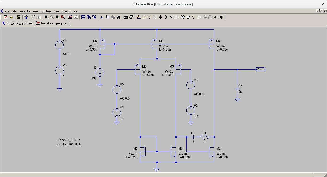 I understand that I could do some transistor sizing to change resistance, therefore current. Could you anyone tell me more about it with respect to the spec? Besides, I have tried to test some of the spec. But I still do not understand how to test some of them especially Input Common Mode Range, Output Swing, Power Suppy Rejection Ratio, Common Mode Rejection at DC. |
|
|
|
« Last Edit: March 01, 2016, 03:42:31 03:42 by promach »
|
Logged
|
|
|
|
|
|
Vineyards
Active Member
Offline
Posts: 168
Thank You
-Given: 62
-Receive: 37
|
|
« Reply #16 on: March 01, 2016, 12:50:08 12:50 » |
|
As for PSSR, change the supply voltage between the maximum value of the signal plus a few volts to the maximum VDD and VSS voltages calculate the ratio between the change in the output voltage and the actual supply voltages. Ideally there must be no variation on the output voltage as the supply voltage changes
Posted on: March 01, 2016, 01:47:38 13:47 - Automerged
To test common mode rejection you should apply the same voltage to the inverting and non inverting inputs any output value other than zero is a deviation from the ideal opamp spec. However, you should first take into account deviations caused by other factors and offset them.
|
|
|
|
|
Logged
|
|
|
|
promach
Junior Member
Offline
Posts: 44
Thank You
-Given: 14
-Receive: 0
|
|
« Reply #17 on: March 12, 2016, 09:28:16 09:28 » |
|
I am now working on testing DC small signal gain and unity gain bandwidth. Why would decreasing the value of the ideal current source (I1) will increase the AC open loop gain ? Why would changing values of C1 will change the unity gain bandwidth ? Besides, I would like to generate all the biases without using ideal current source. Do you think it is possible with an addition of one extra transistor ? Posted on: March 06, 2016, 09:20:53 09:20 - Automerged
for settling time check, I have developed an oscillator which is not acceptable at all. Could you advise where I should start debugging ? Thanks a lot !!!  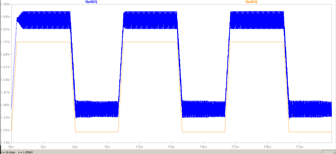  |
|
|
|
|
Logged
|
|
|
|
solutions
Hero Member
Offline
Posts: 1823
Thank You
-Given: 655
-Receive: 900
|
|
« Reply #18 on: March 13, 2016, 05:39:51 05:39 » |
|
What kind of crap school are you going to where they don't teach you enough fundamental material so as to complete a basic project? The reason I ask for its name is so I don't accidentally send my kids there  I don't suppose you've heard the old saw: if you need an oscillator, design an amplifier |
|
|
|
« Last Edit: March 13, 2016, 05:42:07 05:42 by solutions »
|
Logged
|
|
|
|
vern
V.I.P
Active Member
Offline
Posts: 144
Thank You
-Given: 7
-Receive: 41
|
|
« Reply #19 on: March 13, 2016, 11:13:09 11:13 » |
|
"for settling time check, I have developed an oscillator which is not acceptable at all.
Could you advise where I should start debugging ? for a starter try to remove C1 500f (is it 500 Farad?)  |
|
|
|
|
Logged
|
|
|
|
promach
Junior Member
Offline
Posts: 44
Thank You
-Given: 14
-Receive: 0
|
|
« Reply #20 on: March 14, 2016, 07:59:07 07:59 » |
|
Thanks for your help. I have already fulfill DC small signal gain and unity gain bandwidth, with phase margin lacks 5 more degrees. Any advise ? Should I move the zero to the left or right ? How would I do it ?
Besides, I search for CMRR test circuit. I am quite confused with which one to use. Do I need to take into account of offset voltage ?
Could you guys recommend a test circuit for CMRR ?
|
|
|
|
|
Logged
|
|
|
|
promach
Junior Member
Offline
Posts: 44
Thank You
-Given: 14
-Receive: 0
|
|
« Reply #21 on: March 20, 2016, 07:32:21 07:32 » |
|
When I measure output swing for the opamp, I found out that my second gain stage has some problem. I suspect it could the second gain stage bias current. So, I put an ideal current source in series with the second gain stage pmos load M5. However, it has to be at least 19mA for a 1.6V swing. There is something wrong in the second gain stage. But I am stuck when I try to solve it. Please find below the circuit and the output swing result.  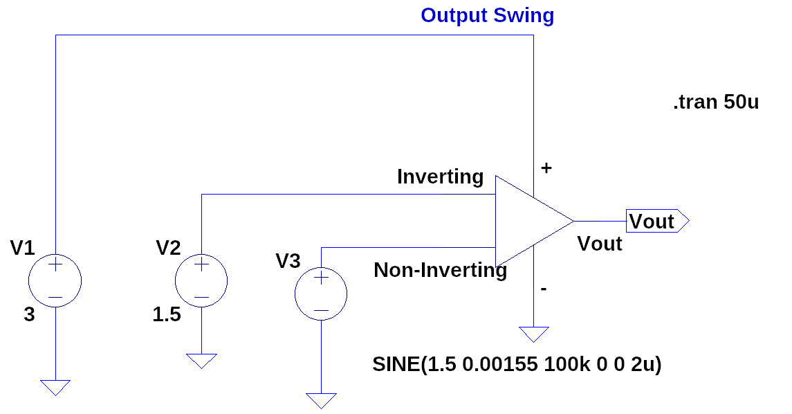  |
|
|
|
|
Logged
|
|
|
|
Signal
Active Member
Offline
Posts: 197
Thank You
-Given: 111
-Receive: 81
|
|
« Reply #22 on: March 21, 2016, 08:22:46 20:22 » |
|
There is no negative feedback on DC that can set an operating point of M6 automatically on that schematics. It looks like M6 is oversaturated by doubled offset made by cascode mirror. By the way, think about how input voltage offset (a pretty standard parameter) of real operational amplifiers reveals itself in case of shorted inputs as you did.
|
|
|
|
|
Logged
|
Give a right name to a right game and play it right
|
|
|
promach
Junior Member
Offline
Posts: 44
Thank You
-Given: 14
-Receive: 0
|
|
« Reply #23 on: March 25, 2016, 02:13:33 14:13 » |
|
Dear Signal,
Thanks a lot for your input. I have actually solved the problem by removing additional cascode current mirror.
What I do not understand is :
a) What do you mean by no negative feedback on DC ?
b) What do you mean by double offset ?
c) How do I relate this problem to the input voltage offset ?
I want to push for more gain beyond what I have now in the schematics.
I try to change some of the parameters of the mosfets without success.
Could you suggest ?
|
|
|
|
|
Logged
|
|
|
|
Signal
Active Member
Offline
Posts: 197
Thank You
-Given: 111
-Receive: 81
|
|
« Reply #24 on: March 25, 2016, 08:30:08 20:30 » |
|
a) What do you mean by no negative feedback on DC ?
Does it mean that you do not understand term "negative feedback"? Or do you see negative feedback in the circuit that generated last waveforms? Or course there are some, can you enumerate them (not here not for me)? Is there one that sets an appropriate bias for M6 transistor? b) What do you mean by double offset ?
Two current mirrors in stack, each of them having its offset ... Am I wrong in terms? (I'm not native English) c) How do I relate this problem to the input voltage offset ?
Imperfection of opamp or variation of parameters could be seen also as input offset. In your case adding an input offset could decrease voltage on M6-gate. But there is a "tradeoff" in your circuit - most likely a voltage on M8 drain that is good for proper bias of M6 is not enough for M3-M4-M8-M9 mirror to work properly. Hard task to adapt these values, isn't it? I mentioned an input offset because I think that someone that designs an opamp should be fluent with this and the output waveform looks like the output of untrimmed opamp (that is ok). I want to push for more gain beyond what I have now in the schematics.
I try to change some of the parameters of the mosfets without success.
Could you suggest ?
It looks like you are not ready to think about treated circuit it terms of "current source", "current mirror", "differential amplifier", etc. . You miss the stage of studying each of these blocks in terms of "transistor", "bias", "currentvoltage characteristic", "transfer characteristic", "feedback" etc.. Also it looks like you heard that cascode mirror as a load of differential amplifier increases gain compared to basic mirror (was it a suggestion made by someone before?), but do not understand why and why it could be not so great. Even if you heard that it is due to greater impedance I am not sure that it is clear for you. Taking for granted the balanced circuit of DC amplifier you changed one block and ask what's wrong with second gain stage. One answer could be - you forgot about bias. But better answer - I's just because you think about electronics as a magic. Or course it's magic, but you are supposed to be a magician, and tricks of "some parameters" is not enough for magic. I do not want to suggest particular things. You need to attend all series of lectures and read all connecting materials/books, thinking in terms "what is going on" instead of "what I should remember". Forum is not a book nor lecture. You definitely should read books, and you definitely did not read enough of them. |
|
|
|
|
Logged
|
Give a right name to a right game and play it right
|
|
|
promach
Junior Member
Offline
Posts: 44
Thank You
-Given: 14
-Receive: 0
|
|
« Reply #25 on: March 26, 2016, 04:26:14 04:26 » |
|
Dear Signal, I am sorry due to my limited knowledge in analog electronics.
I actually missed the most important stage which you have said.
I have not taken many courses that deal with circuit calculation and analysis.
I go to school to learn more about theoretical electronics.
|
|
|
|
|
Logged
|
|
|
|
|


